- 您现在的位置:买卖IC网 > Sheet目录3887 > PIC24F04KL101-I/SS (Microchip Technology)IC MCU 16BIT 4KB FLASH 20-SSOP
CHAPTER 4 PORT FUNCTIONS
User’s Manual U15905EJ2V1UD
112
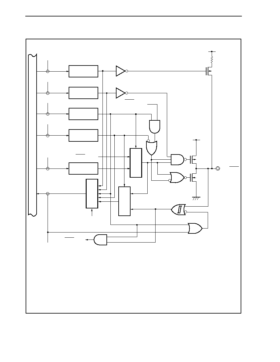
Figure 4-10. Block Diagram of P32
Internal
bus
WRPMC
RD
Address
SCK1 output
SCK1 input
SCK1 output
enable signal
WRPORT
P32/SCK1
PMC32
Selector
WRPU
PU32
WRPM
PM32
Output latch
(P32)
WRPF
PF32
PMC3
PU3
PM3
P3
PF3
EVDD
P-ch
EVDD
EVSS
P-ch
N-ch
Caution
This pin does not have hysteresis characteristics in the port mode.
It has hysteresis characteristics only when an input-pin alternate function is used.
Remark
P3:
Port register 3
PM3:
Port mode register 3
PMC3: Port mode control register 3
PFC3: Port function control register 3
PU3:
Pull-up resistor option register 3
发布紧急采购,3分钟左右您将得到回复。
相关PDF资料
PIC16HV540-04/P
IC MCU OTP 512X12 18DIP
PIC16C54C-04/P
IC MCU OTP 512X12 18DIP
22-02-3093
CONN FFC/FPC VERTICAL 9POS .100
PIC16C620A-04/P
IC MCU OTP 512X14 COMP 18DIP
PIC16F722-I/SP
IC PIC MCU FLASH 2KX14 28-DIP
PIC16F684-I/P
IC PIC MCU FLASH 2KX14 14DIP
PIC16LC782T-I/SO
IC MCU OTP 2KX14 A/D D/A 20SOIC
PIC18LC601T-I/PT
IC MCU ROMLESS A/D PWM 64TQFP
相关代理商/技术参数
PIC24F04KL101T-I/MQ
功能描述:16位微控制器 - MCU 4KB FLASH 512B RAM 18 I/O 10-BIT ADC RoHS:否 制造商:Texas Instruments 核心:RISC 处理器系列:MSP430FR572x 数据总线宽度:16 bit 最大时钟频率:24 MHz 程序存储器大小:8 KB 数据 RAM 大小:1 KB 片上 ADC:Yes 工作电源电压:2 V to 3.6 V 工作温度范围:- 40 C to + 85 C 封装 / 箱体:VQFN-40 安装风格:SMD/SMT
PIC24F04KL101T-I/SO
功能描述:16位微控制器 - MCU 4KB FLASH 512B RAM 18 I/O 10-BIT ADC RoHS:否 制造商:Texas Instruments 核心:RISC 处理器系列:MSP430FR572x 数据总线宽度:16 bit 最大时钟频率:24 MHz 程序存储器大小:8 KB 数据 RAM 大小:1 KB 片上 ADC:Yes 工作电源电压:2 V to 3.6 V 工作温度范围:- 40 C to + 85 C 封装 / 箱体:VQFN-40 安装风格:SMD/SMT
PIC24F04KL101T-I/SS
功能描述:16位微控制器 - MCU 4KB FLASH 512B RAM 18 I/O 10-BIT ADC RoHS:否 制造商:Texas Instruments 核心:RISC 处理器系列:MSP430FR572x 数据总线宽度:16 bit 最大时钟频率:24 MHz 程序存储器大小:8 KB 数据 RAM 大小:1 KB 片上 ADC:Yes 工作电源电压:2 V to 3.6 V 工作温度范围:- 40 C to + 85 C 封装 / 箱体:VQFN-40 安装风格:SMD/SMT
PIC24F08KA101
制造商:MICROCHIP 制造商全称:Microchip Technology 功能描述:Flash Programming Specifications
PIC24F08KA101-E/MQ
功能描述:16位微控制器 - MCU 8KB15KB RAM 512B EE SERIAL EE IND RoHS:否 制造商:Texas Instruments 核心:RISC 处理器系列:MSP430FR572x 数据总线宽度:16 bit 最大时钟频率:24 MHz 程序存储器大小:8 KB 数据 RAM 大小:1 KB 片上 ADC:Yes 工作电源电压:2 V to 3.6 V 工作温度范围:- 40 C to + 85 C 封装 / 箱体:VQFN-40 安装风格:SMD/SMT
PIC24F08KA101-E/P
功能描述:16位微控制器 - MCU 8KB15KB RAM 512B EE SERIAL EE IND RoHS:否 制造商:Texas Instruments 核心:RISC 处理器系列:MSP430FR572x 数据总线宽度:16 bit 最大时钟频率:24 MHz 程序存储器大小:8 KB 数据 RAM 大小:1 KB 片上 ADC:Yes 工作电源电压:2 V to 3.6 V 工作温度范围:- 40 C to + 85 C 封装 / 箱体:VQFN-40 安装风格:SMD/SMT
PIC24F08KA101-E/SO
功能描述:16位微控制器 - MCU 8KB15KB RAM 512B EE SERIAL EE IND RoHS:否 制造商:Texas Instruments 核心:RISC 处理器系列:MSP430FR572x 数据总线宽度:16 bit 最大时钟频率:24 MHz 程序存储器大小:8 KB 数据 RAM 大小:1 KB 片上 ADC:Yes 工作电源电压:2 V to 3.6 V 工作温度范围:- 40 C to + 85 C 封装 / 箱体:VQFN-40 安装风格:SMD/SMT
PIC24F08KA101-E/SS
功能描述:16位微控制器 - MCU 8KB15KB RAM 512B EE SERIAL EE IND RoHS:否 制造商:Texas Instruments 核心:RISC 处理器系列:MSP430FR572x 数据总线宽度:16 bit 最大时钟频率:24 MHz 程序存储器大小:8 KB 数据 RAM 大小:1 KB 片上 ADC:Yes 工作电源电压:2 V to 3.6 V 工作温度范围:- 40 C to + 85 C 封装 / 箱体:VQFN-40 安装风格:SMD/SMT